|
|
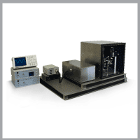
The Kelvin Probe
The Kelvin Probe is a non-contact,
non-destructive vibrating capacitor device
used to measure the work function (wf) of
conducting materials or surface potential (sp) of
semiconductor or insulating surfaces. The wf of a
surface is typically defined by the topmost 1-3 layers
of atoms or molecules, so the Kelvin Probe is one of
the most sensitive surface analysis techniques available.
KP Technology Systems offer very high wf resolution of
1-3 meV, currently the highest achieved by any commercial device.
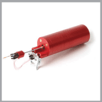
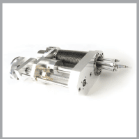
The Kelvin Probe does not actually touch the surface; rather an electrical contact is made to another part of the sample or sample holder. The probe tip is typically 0.2 - 2.0 mm away from the sample and it measures the 'traditional work function', i.e. that found in literature tables. Other techniques, using very sharp tips some 10's of nanometers away from the sample, measure very reduced and distorted work functions due to the close separation of tip and sample.
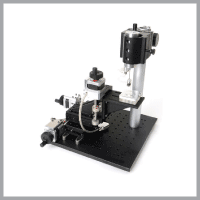
The physical form of a Kelvin Probe is a head unit containing a voice coil driving system and integral amplifier suspended above a sample. The vibrating tip and the sample forms a capacitor, having ideal, or parallel-plate, geometry. As the tip vibrates electric charge is pushed around the external detection circuit. By careful control of the tip potential and automatic capture and analysis of the resulting waveform both the potential across the capacitor and the capacitor spacing can be calculated to very high resolution. In scanning form the tip is steered across the sample surface using a high resolution 3-axis translator. The spatial resolution of the tip is approximately the tip diameter, we typically use tips of 2 and 0.05 mm as standard tips in air and anything from a sharp tip to 10 mm diameter in Ultrahigh Vacuum. The resulting 3D surface work function images contain information about surface structures, surface composition, thin films, defects, etc. In time-varying mode artifacts such as oxidation (corrosion), defect relaxation, etc can be observed.
For semiconductor surfaces, both organic (Polymer) and inorganic (Si, Ge, CdS, etc) the Kelvin Probe is the only way to directly measure the Fermi-level. Changes in fermi-level, caused by illumination with white or monochromatic light, results in energy band shifts which can be used to characterize interface and bulk defect states. These techniques are termed Surface Photovoltage (SPV) and Surface Photovoltage Spectroscopy (SPS) for which KP Technology can supply both software and accessories for our systems.
The Traditional Kelvin Probe actually produces the work function difference between the tip and sample. The kelvin method was first postulated by the renowned scottish scientist Lord Kelvin, in 1861. Typically the tip is calibrated against a reference surface, such as gold first. However KP Technology is the only company to offer absolute Kelvin Probes, which combine the Kelvin method and Einstein Photoelectric effect to produce absolute work function values (in eV).
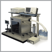
KP Technology has developed dedicated head units for ambient, controlled atmosphere, relative humidity and ultrahigh vacuum environments. All of our systems share the OFF-Null, Height Regulation (ONHR) method invented by Prof. Baikie and consequently produce stable high signal levels, repeatable and high- resolution measurements. The rapid growth of the company since 2000 means the KP Technology Systems are found in leading materials research laboratories worldwide. We pride ourselves on our rapid post-sales support and our ability to assist technical and data interpretation queries.
Back to What is...
|
| |
|
|
 |